6-Layer PCB Design for Analog Satellite Control System
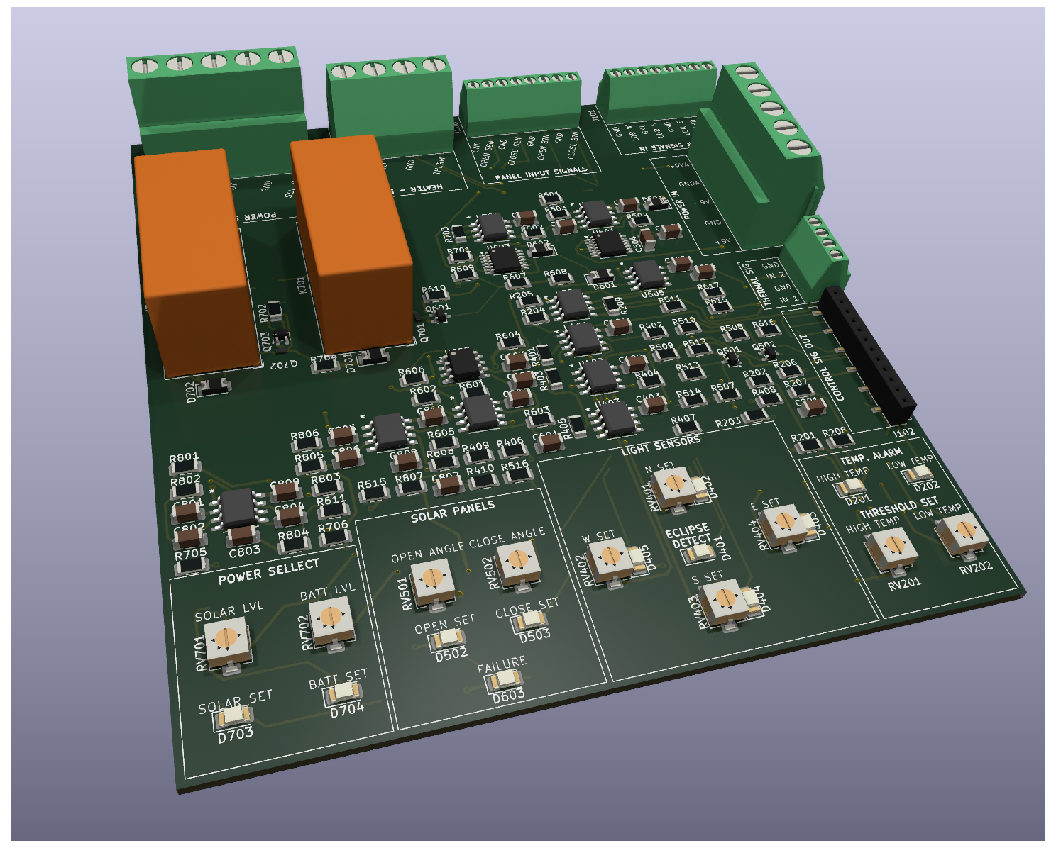
3D render of main PCB - the analog brain of the satellite control system
Project Repository:
https://github.com/SimonAulet/portfolio/tree/main/PCBContains all project files: KiCad schematics, PCB designs, LTSpice simulations, datasheets, and component libraries for direct import.
Context
Group development of an analog satellite control system implemented with discrete components. The system integrates orientation detection through photoresistors, thermal sensing, analog PWM generation, servomotor positioning, timing circuits, analog latches, and autonomous control logic.
My Contribution
Comprehensive KiCad Design: Integration and physical development of the system from laboratory-implemented modules. This involves creating the unified schematic in KiCad, strategic selection of components compatible with industrial assembly, footprint and 3D model management, implementation of design classes for signal separation (analog, digital, power), critical routing, and exhaustive validation through ERC/DRC, culminating in a 6-layer PCB ready for manufacturing.
Analog Simulation and Validation: LTSpice simulation of key stages: hysteresis comparators (Schmitt trigger), analog PWM generator, timing circuits, decision logic for power source switching via relays, and latches implemented with NPN transistors.
Phase 1: Architecture
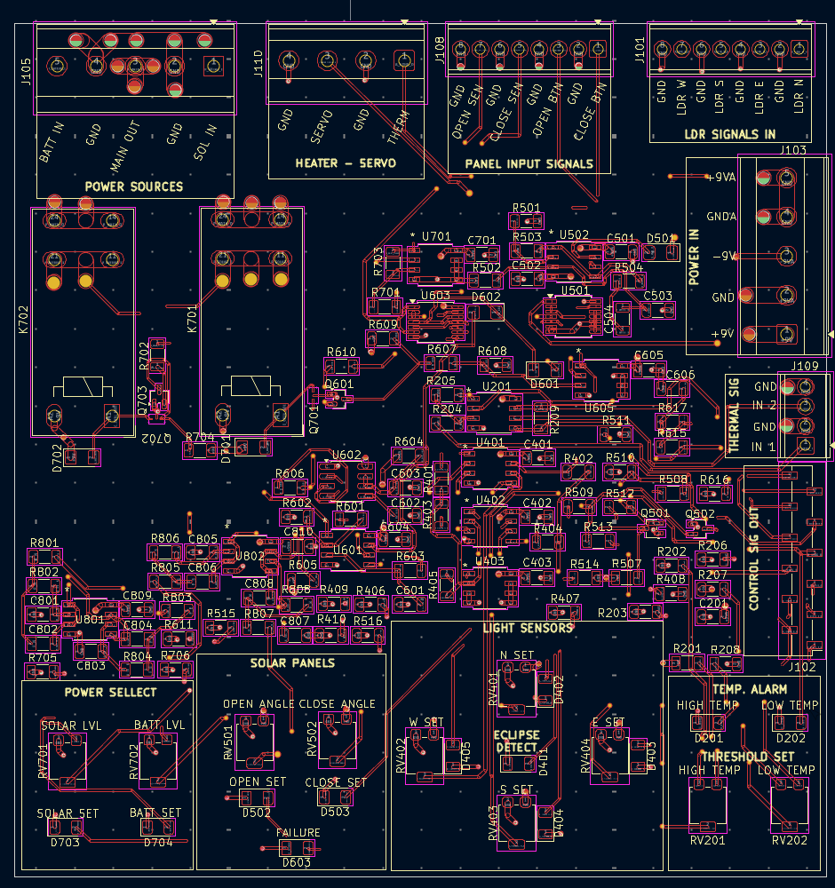
General System

Main schematic sheet - organized as interconnection map between subsystems
The design was structured into 6 modular subsheets, each encapsulating a specific function:
- Active filtering for LDR sensor signal conditioning
- Orientation sensing for eclipse/position detection
- Thermal control with LM35 sensing and actuation
- Solar panel deployment with PWM control and verification
- Deployment verification using 555 timers
- Power source selector for automatic switching between solar/battery
Communication between modules was established through coherently named signals using prefixes. For example A_ → Sensitive analog signals, C_ → Commands and control signals, F_ → Feedback, L_ → LED indicators, etc. and suffixes to indicate input (_I) or output (_O)
Detailed Schematics
Complete system schematics with all components and detailed connections.
Format: Interactive PDF · Content: Complete schematics
Download Schematics (PDF)Component Selection
Each component was chosen considering electrical specifications, availability, layout implications, and thermal/mechanical requirements. We attempted to use all from the same manufacturer (Texas Instruments) when possible:
| Component | Manufacturer | Key Features | Selection Reason |
|---|---|---|---|
| LM35 | Texas Instruments | Sensor de temperatura, TO-220 | Allows direct screwing to batteries/heat sources for precise measurement |
| LM358B | Texas Instruments | Op-amp dual, SMD, 0.1µF en Vcc | Proven stability, integrated compensation, compact package |
| CSD17577Q5A | Texas Instruments | MOSFET N-ch, 25V, 6.7mΩ | Switching efficiency, low Rds(on), optimal for relays |
| RT314009 | TE Connectivity | Relay 9V/16A, 1 Forma C | Current capacity for battery switching, coil compatible with 9V |
Layout considerations: SMD packages were prioritized to reduce parasitic inductances, while components like the LM35 in TO-220 located in external sensors allowed robust mechanical mounting where direct thermal transfer was required.
Phase 2: Physical Implementation - 6-Layer PCB
Stackup Strategy
The 6-layer distribution was optimized to ensure signal integrity and facilitate debugging, with clear function separation:
| Layer | Designation | Main Content | Key Consideration |
|---|---|---|---|
| 1 | F.Cu (Top) | Critical analog signals | Accessible for measurement, short traces |
| 2 | In1.Cu | Continuous ground plane | Low impedance reference |
| 3 | In2.Cu | Power distribution | Separation between clean and general power |
| 4 | In3.Cu | Control signals and setpoints | Isolation from analog paths |
| 5 | In4.Cu | Interconnections and LEDs | Utility layer |
| 6 | B.Cu (Bottom) | Long-distance analog routes | "Highways" with predictable routing |
Layer Visualization
F.Cu + In1.Cu
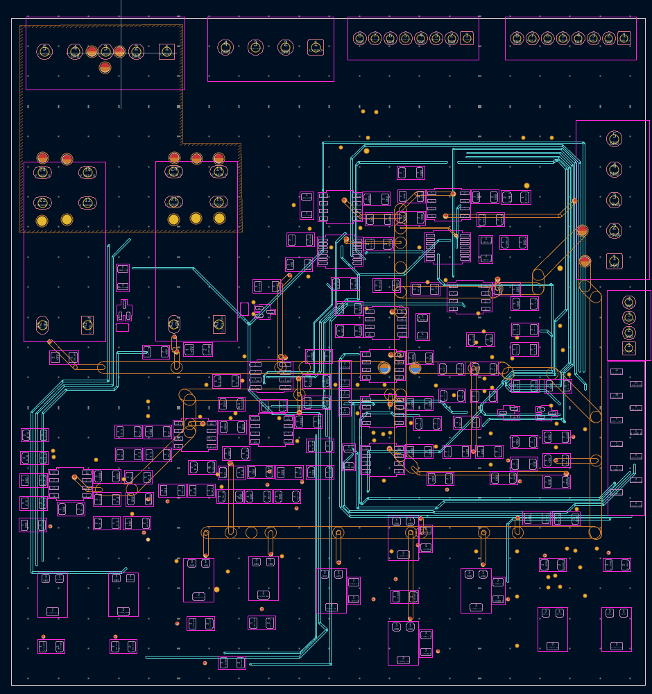
In2.Cu + In3.Cu
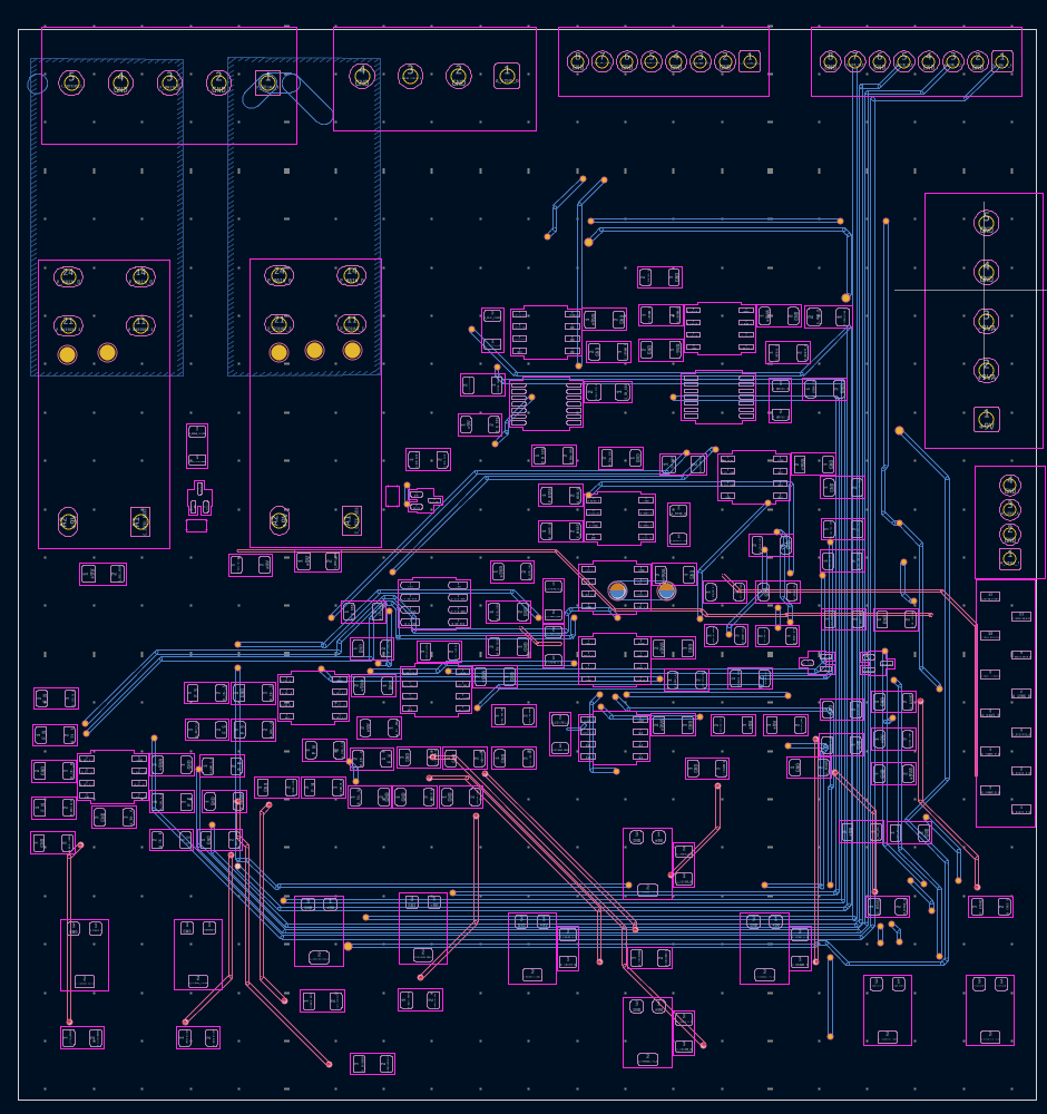
In4.Cu + B.Cu
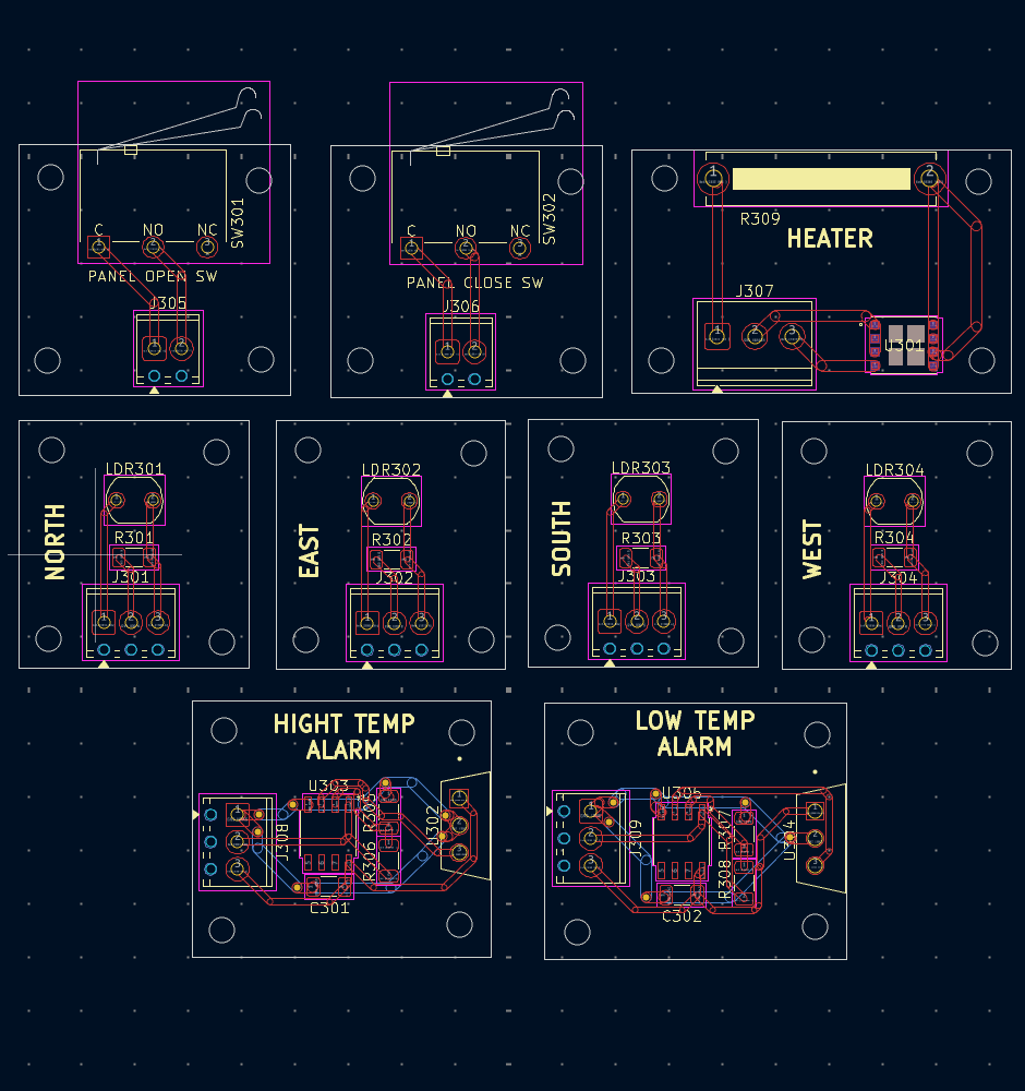
Sensory Modules
Routing Methodology
Routing followed a strict hierarchy, prioritizing integrity over convenience:
- Ground - Reference establishment with multiple vias
- Power - Traces dimensioned according to required current. Separation of IC power (
power_clean) from general power - Feedback signals - Direct and protected routes
- Analog signals - Length minimization and crossing avoidance
- Control and LEDs - Completion of interconnections
This sequence ensured that the most sensitive signals had optimal routes before compromising space with secondary functionalities.
External Subsystems and Connectivity
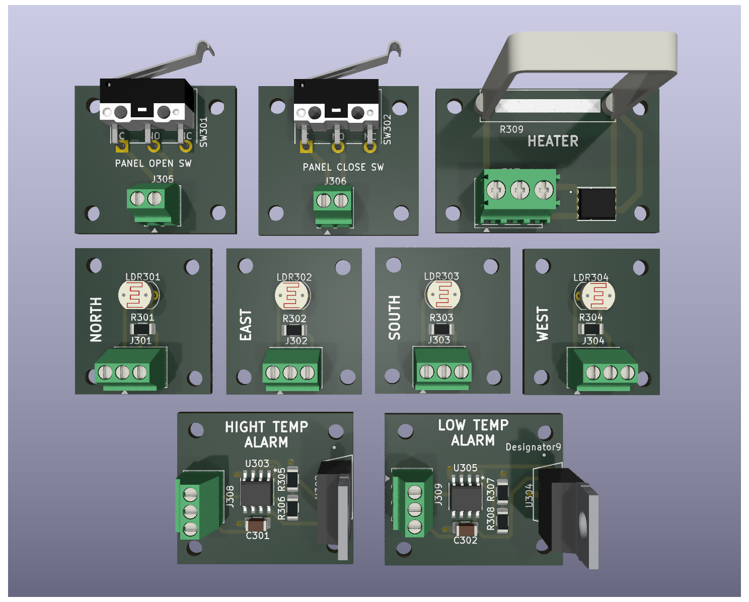
Distributed sensors and actuators - modular solution with clearly identified connectivity
The complete system extends beyond the main PCB through external modules:
- 4 light detection modules, each with 1 LDR for omnidirectional coverage.
- 2 LM35 temperature sensors for thermal monitoring in critical locations.
- 1 heater module activated by the low temperature alert signal.
- 2 limit switches for physical detection of solar panel opening and closing.
Each module is a square double-layer PCB with holes for robust mechanical mounting. Interconnection with the main board is done through cables connected to labeled terminal blocks at both ends, ensuring error-free installation and facilitating maintenance or individual replacement of any subsystem without affecting the whole.
Key Design Points
- Effective domain separation: The 63 signals organized into classes allowed applying consistent and automated design rules.
- Successful hierarchical routing: Starting with reference and power, then critical signals, finally secondary functionalities.
- Built-in debugging: All critical signals accessible on external layers, with space for test points where necessary.
- Exceeded specification compliance: The final design exceeds the minimum clearance and trace width requirements of the selected manufacturer.
Simulation and Analytical Validation
Each critical subsystem of the design was modeled and validated in LTSpice before any physical implementation. Starting from functional requirements —hysteresis comparators, analog latches, timers, and PWM generators— models were built using real components, such as the LM358 opamp configured according to its Texas Instruments datasheet, and PWL signals to simulate operational conditions.
This simulation process allowed optimizing component values, verifying design margins, and predicting system behavior with high accuracy. The results were then successfully correlated with breadboard measurements using a high-end Tektronix oscilloscope, establishing a solid foundation for the final PCB design.
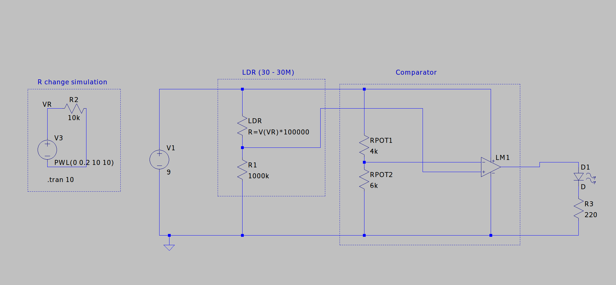
1. Hysteresis Comparator (Schmitt Trigger)
Hysteresis was implemented to eliminate switching oscillations with noisy or slowly varying signals. The circuit was modeled in LTSpice and characterized both analytically and experimentally.
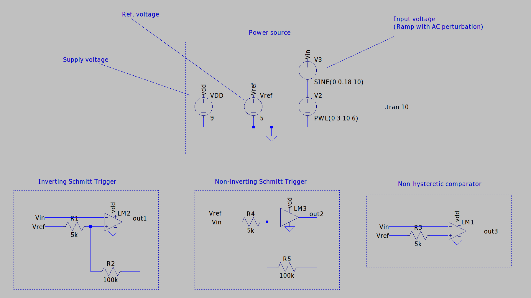
Circuit implemented in LTSpice
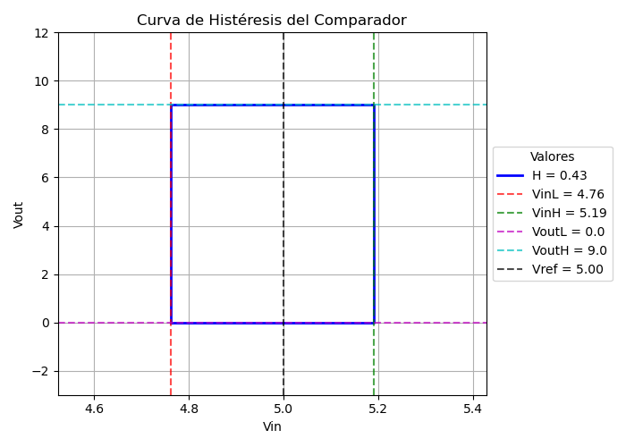
Analytical calculation: H = 0.43 V
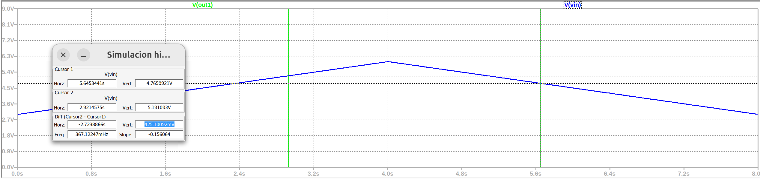
Simulation validation: ΔV = 425 mV between thresholds
The simulation with a triangular ramp confirms that switching occurs with a 425 mV difference between rising and falling edges, in excellent agreement with the theoretical calculation of 430 mV. This ensures noise immunity and stability in threshold detection.
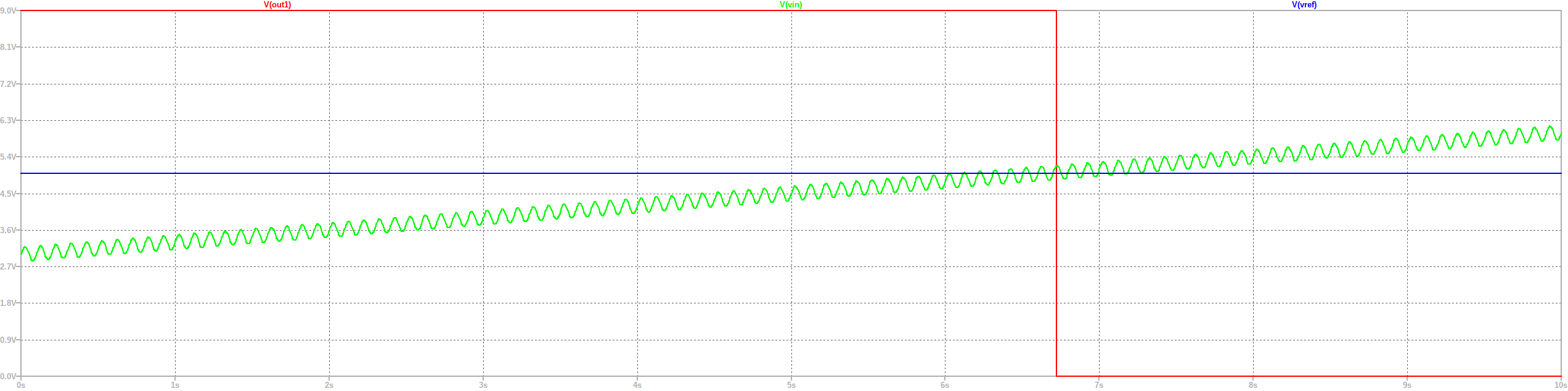
Inverting configuration with noise
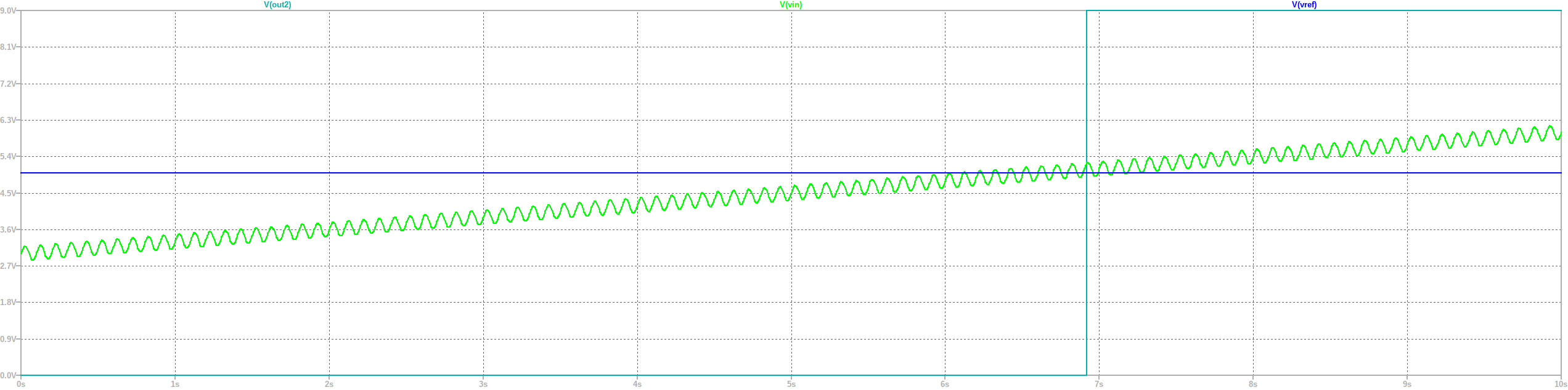
Non-inverting configuration
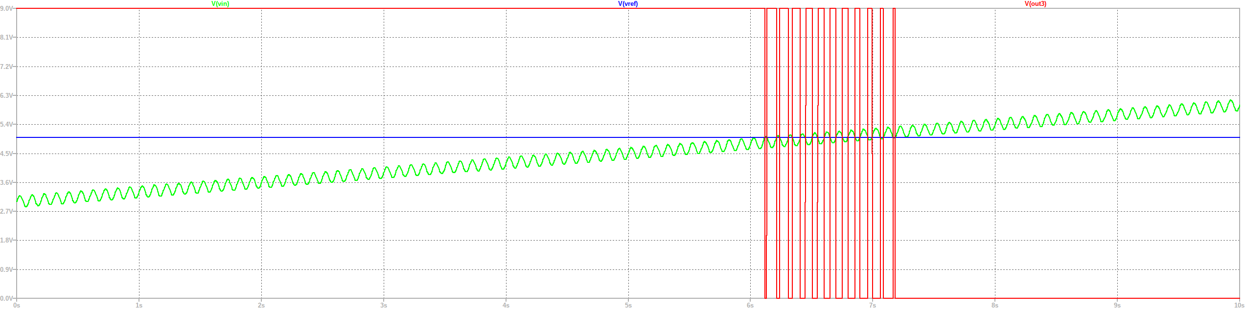
Without hysteresis: oscillations at threshold
The waveforms demonstrate the design's effectiveness: while the comparator without hysteresis shows multiple unwanted switching events when crossing the threshold, both Schmitt trigger configurations maintain a clean and stable output even with noisy input signals.
2. Analog Timing and Alarm Logic
The timing subsystem integrates a 555 timer, a custom anti-latch circuit, and alarm enable logic to ensure error signals activate only under valid conditions.
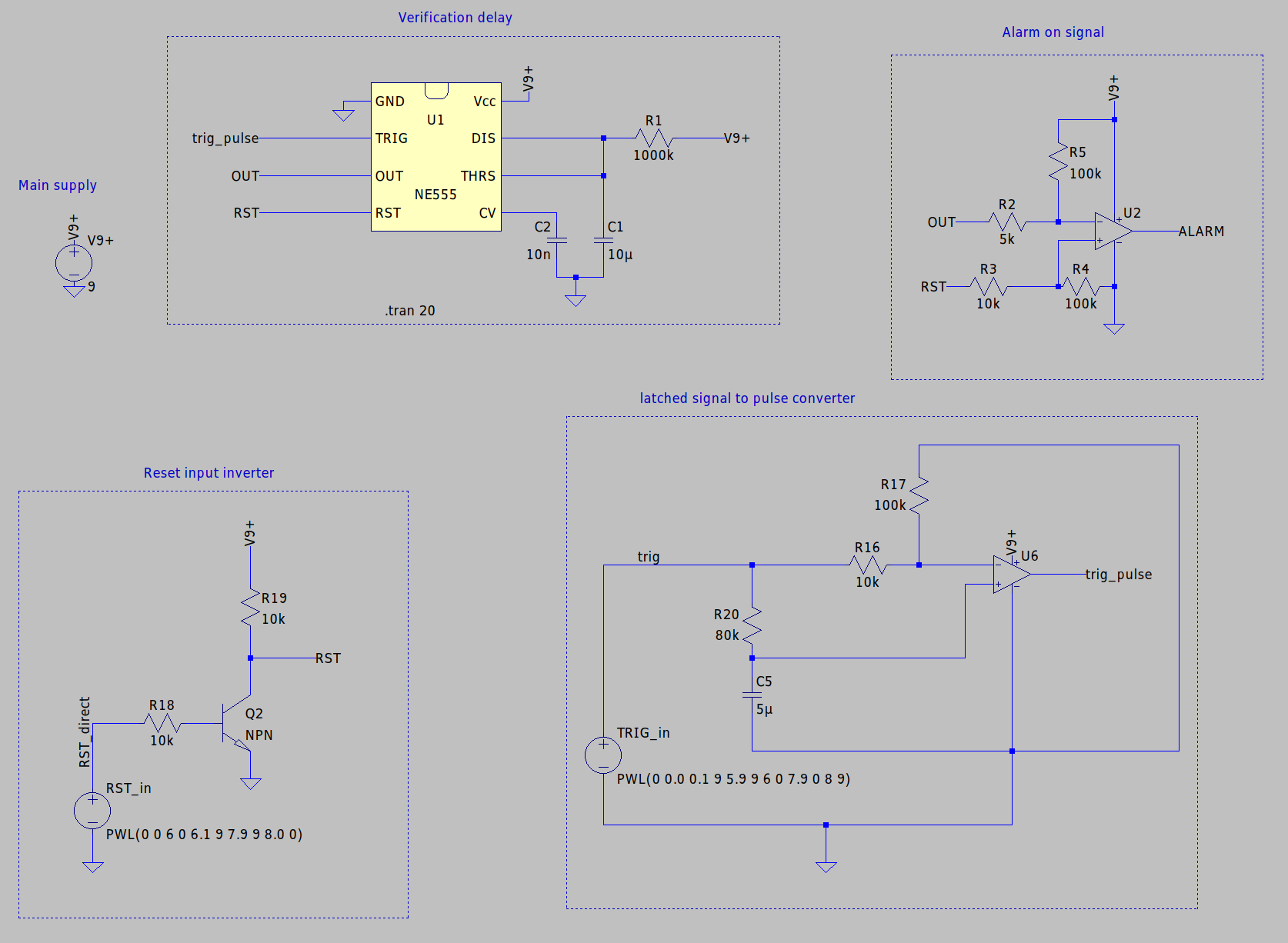
Complete circuit: 555 timer, alarm logic, and latch-to-pulse converter
Latch-to-Pulse Converter
Original design that solves a specific requirement: the 555 needs an edge, not a sustained signal. Implemented with an LM358 and 5 µF capacitor, it generates a short pulse on each rising edge of the input, ignoring its subsequent state. Used twice in the system (for opening and closing panel verification).
.png)
Annotated latch-to-pulse converter - converts continuous signal to activation pulse
555 Timer Behavior
The 555 operates with active-low output. The simulation shows two activation modes: through reset signal (undesired, requiring filtering) and through a valid trigger after the timing period.
.png)
Activation by reset (left) and by valid trigger (right)
Alarm Enable Logic
Implemented with an opamp as comparator, it acts as an analog AND gate to avoid false positives during system reset. Only when the trigger is active (low) and the reset is inactive (high) is the alarm signal generated.
.png)
Analog AND logic: alarm only with active trigger and inactive reset
3. Analog Latch with NPN Transistors
Simple latch implemented with two cross-coupled NPN transistors that maintains a stable state (ON/OFF) until receiving an opposite switching signal. Used to retain the deployment state of solar panels.
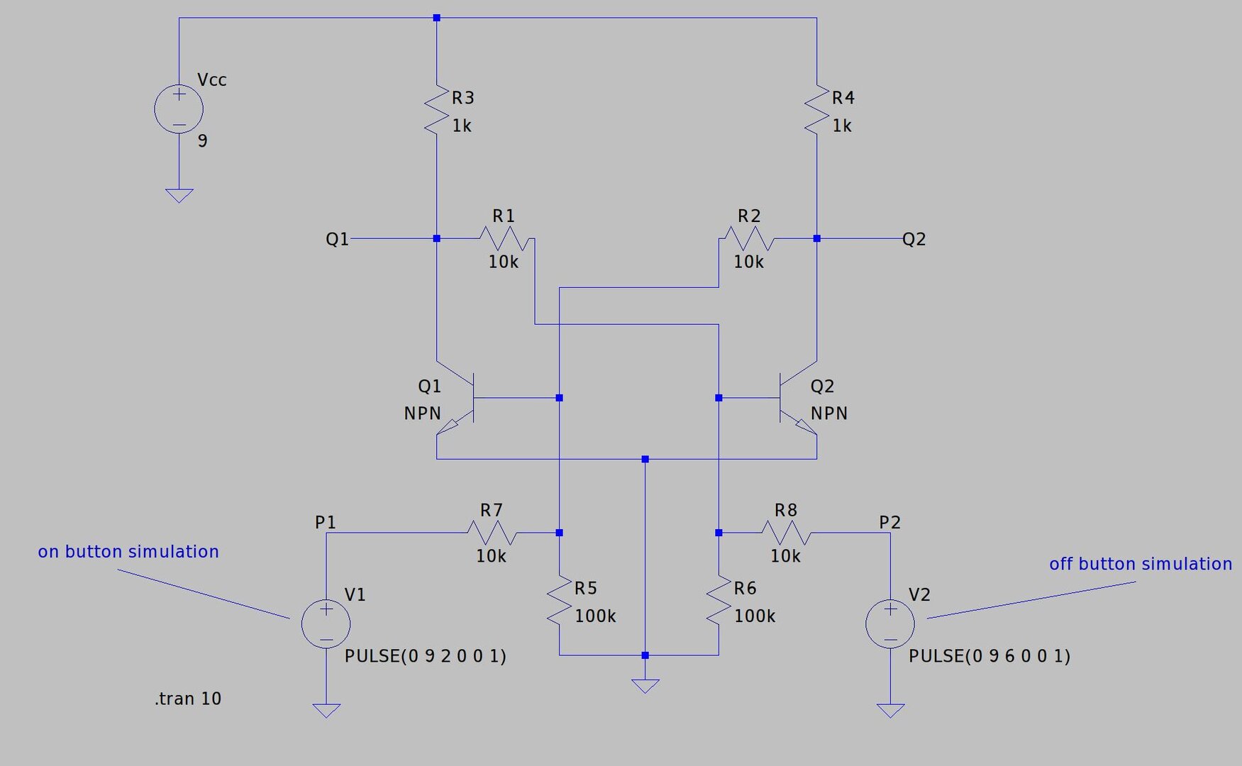
Analog latch: cross-coupled NPN transistor configuration for state retention
.png)
State 1: Q1 active, Q2 inactive - stable output
.png)
State 2: Q2 active, Q1 inactive - clean switching
The latch responds correctly to input pulses, maintaining the last activated state without additional consumption until the next switching. The simulation confirms stable transition between states without oscillations.
4. Power Source Switching with MOSFET
Control stage for relay activation through MOSFETs, managing selection between solar source and batteries. The simulation focuses on MOSFET behavior, as the relay operates as a controlled inductive load.
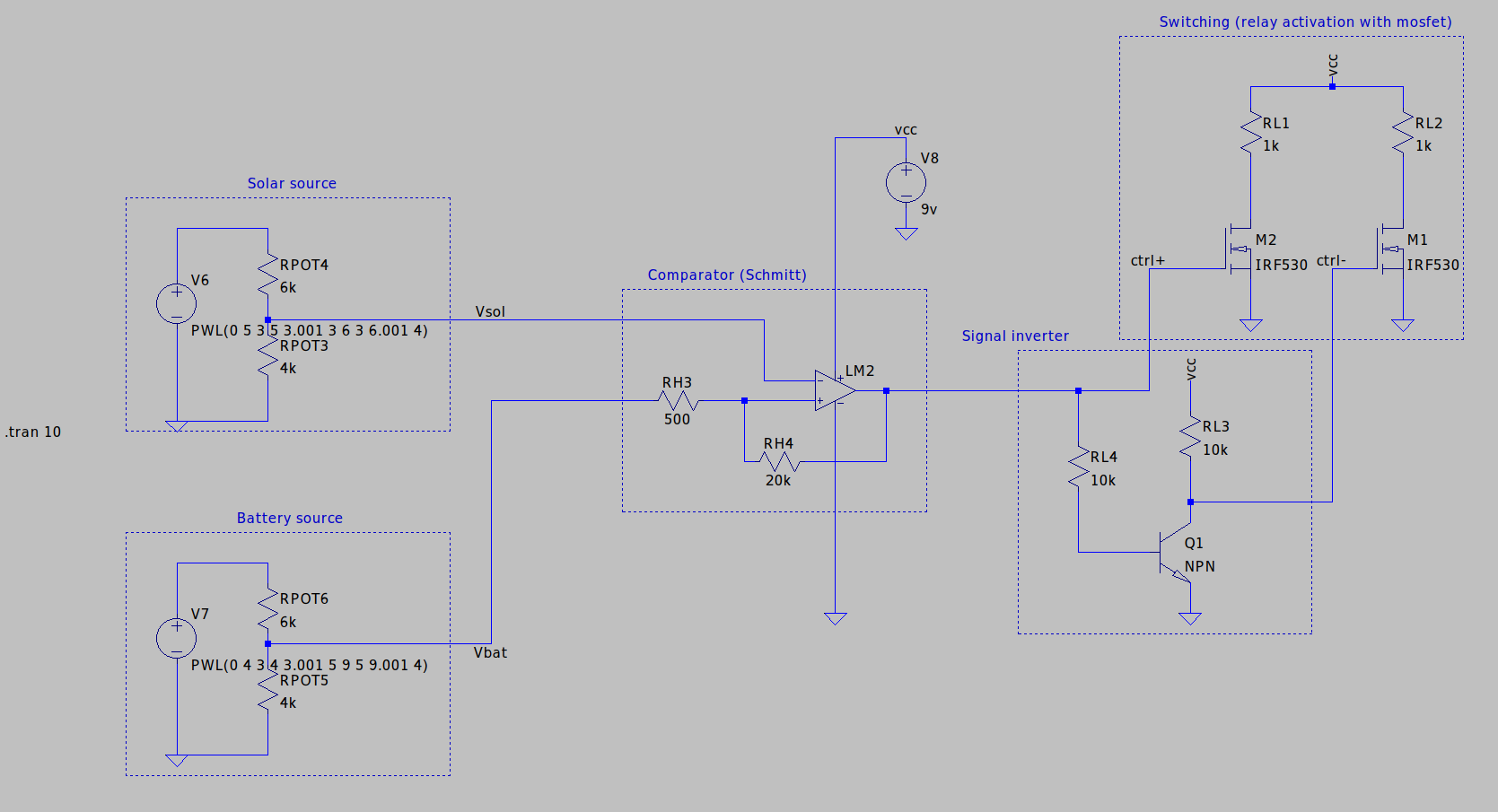
MOSFET driver with protection and control signal from comparator
.png)
Resistive divider with "variable LDR" (PWL-controlled source) and comparator stage
.png)
System response: divider voltage (variable, blue) and comparator output (step, red)
The simulation confirms that the circuit correctly detects when illumination (simulated as variable resistance) crosses the established threshold, generating a clean transition in the comparator output.